UV-LED photolithography exposure |
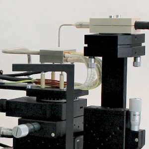
Modular alignment systems |
Infrared (IR) microscope |
HF Vapor Phase Etchers |
Electrostatic chucks |
Wafer chucks for wet processes |
Wafer bonding inspection |
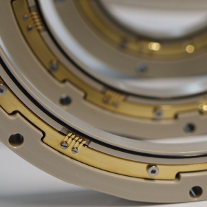
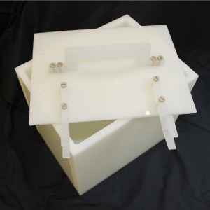
Chip-to-chip anodic bonder |
|
Products
The idonus core products are cleanroom equipment for MEMS microfabrication.
On this page, we have classified these products in two categories of equipment:
- Mask alignment (MAS, DIM ) and photolithography exposure (UV-EXP ), and the combination of both (PLX )
- Systems for MEMS microfabrication (VPE, E-chuck, WPWC, CCB ) and inspection (IR-M, WBI )
Mask aligner and photolithography
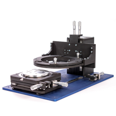
Mask Alignment solutions (MAS )
- Shadow Mask Aligner
- Double Image Microscope (DIM )
- Mask Aligner with DIM (MAS + DIM )
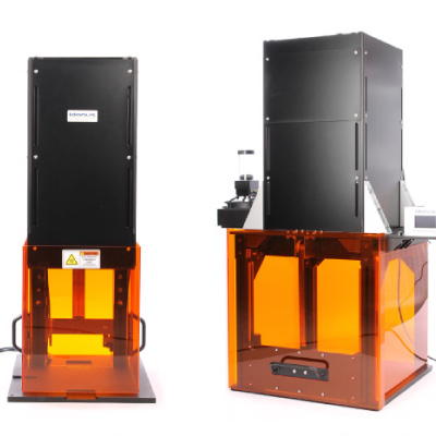
UV-LED Exposure Systems
(UV-EXP series)
A wide range of exposure systems with the UV-EXP series:
- UV-EXP150R: Ø150 mm exposure area
- UV-EXP150S: 150 × 150 mm² exposure area
- UV-EXP200R
- UV-EXP200S
- UV-EXP300S
Entry-level product: UV-LAB100R
Hg-vapor lamp retrofitting and customized designs:
- UV-EXP600S: Very large exposure area 600 × 600 mm² (implies customized design for systemintegration)
- Retrofitting of Hg-based mask aligners
- Customized mounting base using standard UV-EXP products
- Customized design of UV-EXP for other dimensions (e.g., size < 150R)
Photolithography Exposure
(PLX series)
PLX are complete systems combining alignment and UV exposure. The PLX series combines the MAS + DIM with the UV-EXP equipment.
- PLX150: with a UV-EXP150R or UV-EXP150S
- PLX200: with a UV-EXP200R or UV-EXP200S
MEMS microfabrication
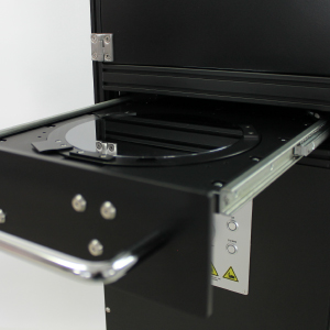
HF Vapor Phase Etcher (VPE series)
VPE series:
- VPE100: up to Ø100 mm wafers
- VPE150
- VPE200
Electrostatic chuck (E-chuck)
Electrostatic clamping of multiple chips or parts of wafers
Wet Process Wafer Chucks (WPWC ) +
Wafer Chuck for Uniform Electrodeposition (WEDC )
Mechanical chucks for wafers chemical etching or for uniform electrodeposition
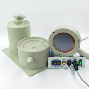
Chip to chip bonder (CCB )
System for the anodic bonding of dies
MEMS inspection
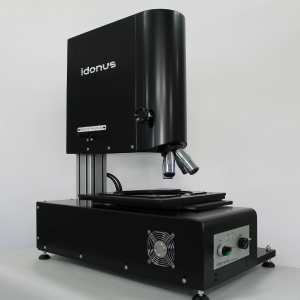
Infrared Microscope (IR-M )
Microscope with IR sensitive camera
Wafer bonding inspection (WBI )
Inspection of full wafers (e.g., after fusion bonding) by means of Infrared (IR) imaging
Other products
- Multiple chip vacuum chuck
- End-of-life (EOF) products are availabe only for clients that had previously purchased these products
Ask for a quotation
Please note that we do not publish any price list online.
If you are interested in one of our products, please contact us to get a quotation (either through one of our sales partners, or directly to our headquarters).
If you feel that one of our standard products would need adaption work to suit your application, please do not hesitate to ask us for advice on engineering work. We can find solutions.
Share this page
Share this URL via e-mail.
idonus sàrl
Rouges-Terres 61
2068 Hauterive / Neuchâtel
Switzerland
Rouges-Terres 61
2068 Hauterive / Neuchâtel
Switzerland

