Infrared Microscope (IR-M )
Silicon wafer is an essential component used in the fabrication of integrated circuits (IC)
and microelectromechanical systems (MEMS). The ability to see through this semiconductor material in the infrared (IR)
range is advantageous for quality control of manufacturing processes.
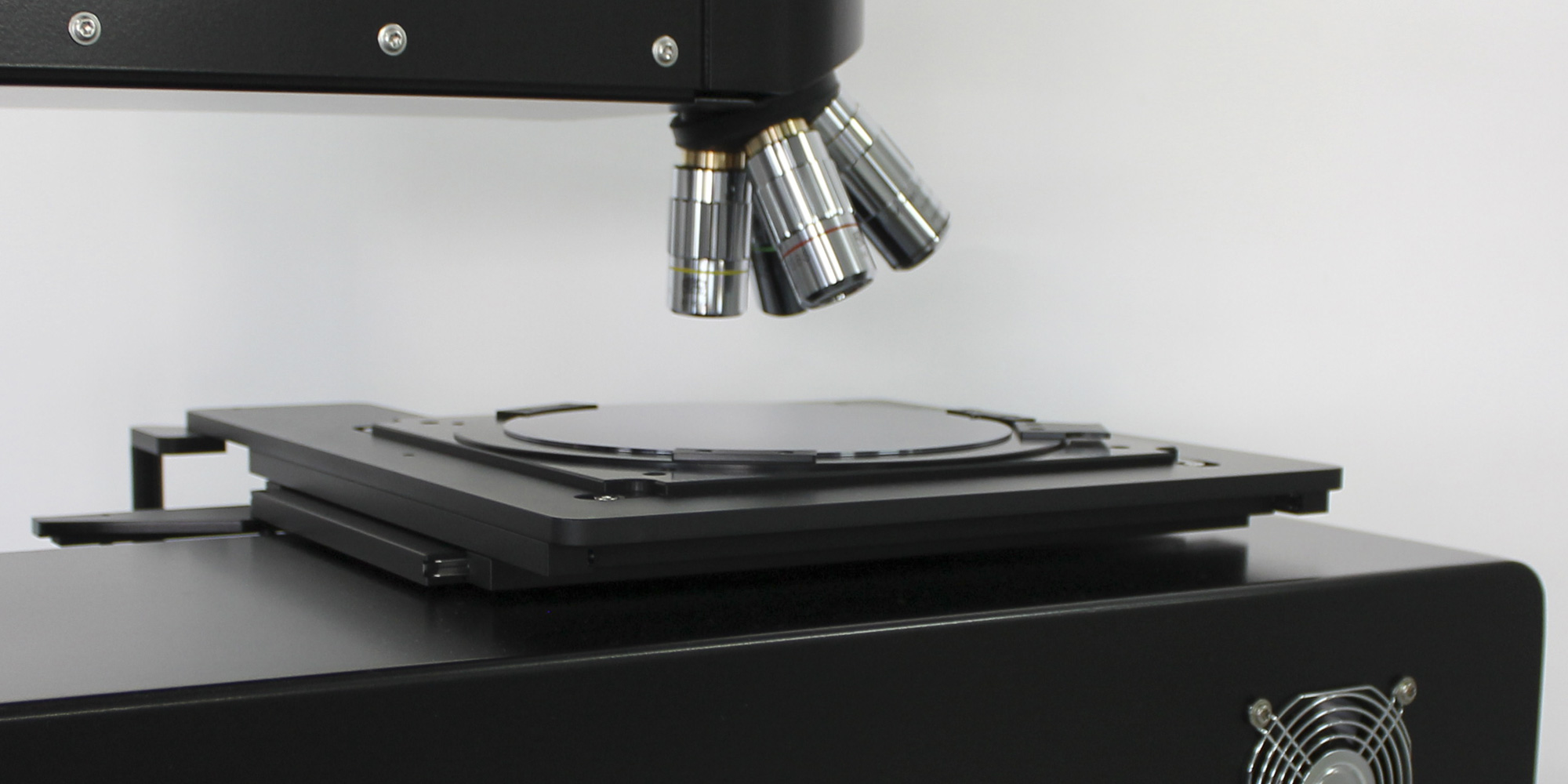
The idonus infrared wafer inspection microscope (IR-M) is equipped with a long working distance objective.
A 3-step zoom allows the user to select the suitable field of view and magnification.
An IR sensitive camera displays the image of the inspected sample on a computer (via USB 3.0 communication).
The resolution is better than 3 μm with a 5× objective.
Additionally, a top side illumination is available.
This allows the microscope to be used in conventional mode and to inspect the top side of the wafer.
The IR microscope is equipped with an xy-table, which accommodates Ø 200 mm (8'') or smaller wafers.
Optionally, the xy-table can be motor driven for convenient controlvia the graphical user interface (GUI) and/or with a joystick.
Download
Download our
IR-M product brochure (
PDF).
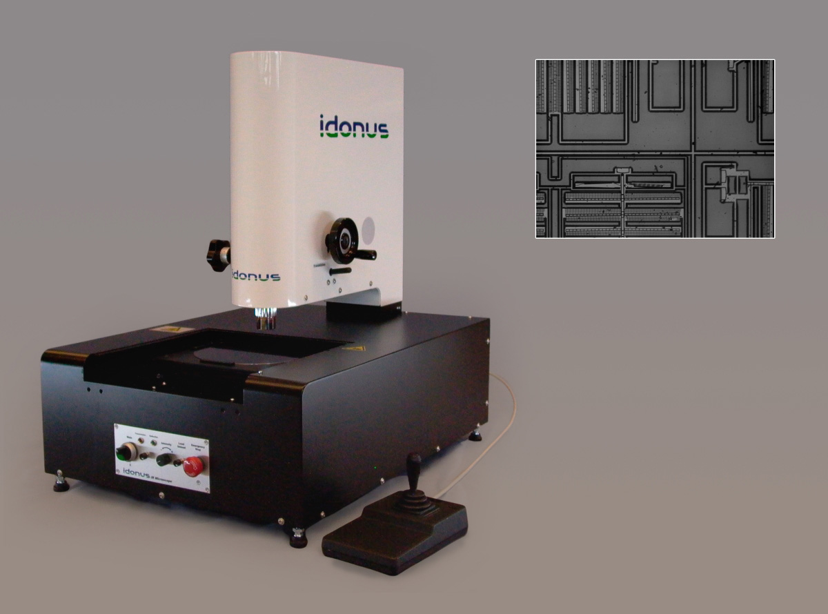
The idonus IR wafer inspection microscope (IR-M) – The version shown includes a motorized xy-stage.
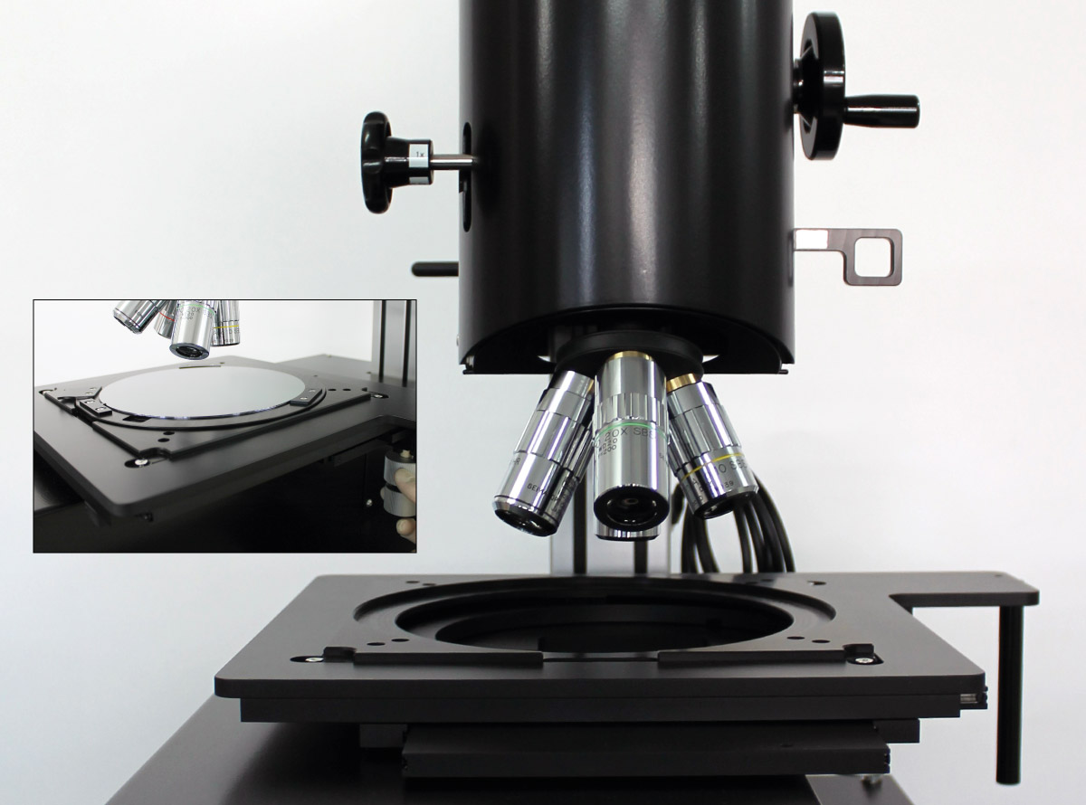
Detail of the idonus IR wafer inspection microscope (IR-M) – The equipment is provided with various wafer holders.
Click on one of the pictures above to see more photographs of the IR-M infrared microscope.
Graphical User Interface (GUI)
A GUI for Windows OS allows the user to operate the microscope with a PC.
It enables complete control of the microscope as well as an automated
acquisition of images on a user defined grid on the wafer.

Applications
The idonus IR-M finds applications, among others, in semiconductor and MEMS devices inspection:
- Observation of silicon wafers by transmission imaging (i.e., microstructured wafers)
- Inspection of the power efficiency of solar cells
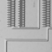
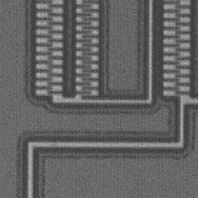
The following images were taken with the IR-M imaging microscope. They show a microstructured
silicon-on-insulator (SOI) wafer. The first image shows the classical microscope image with top side
illumination (visible spectrum). The second image was taken with infrared illumination (IR transmission mode)
and visualizes the buried silicon oxide (SiO2) between the base layer and the device layer.
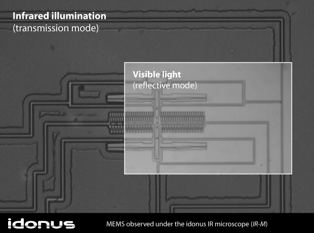
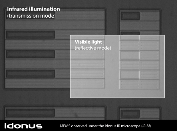
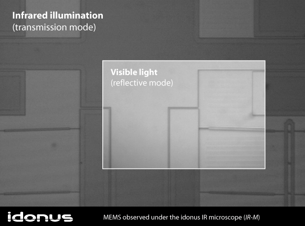
Silicon MEMS device observed under the idonus IR-M infrared microscope –
This illustration shows an IR micrograph (transmission mode) and a superposed picture observed unde visible light (reflection mode).
Click on the illustration above to see more micrographs taken with the idonus IR-M wafer inspection microscope.
|
Useful references
B. R. Simon, "Mode Ordering in Anti-Phase Driven MEMS Gyroscopes and Accelerometers," 2014 (Ph.D. thesis, UC Irivine).
See online PDF document
Fig. B.26 on p. 364 shows micrographs taken with the idonus IR-M for inspection of the buried silicon dioxide layer in a MEMS.
"Fabrication and Testing of a Novel MEMS Rotational Thermal Actuator,"
D. Gee and L. Currano, Report No. ARL-TR-4315 (Adelphi, MD 20783-1197), November 2007.
_01.jpg)
_02.jpg)
_03.jpg)
_04.jpg)
_05.jpg)